
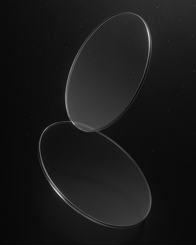
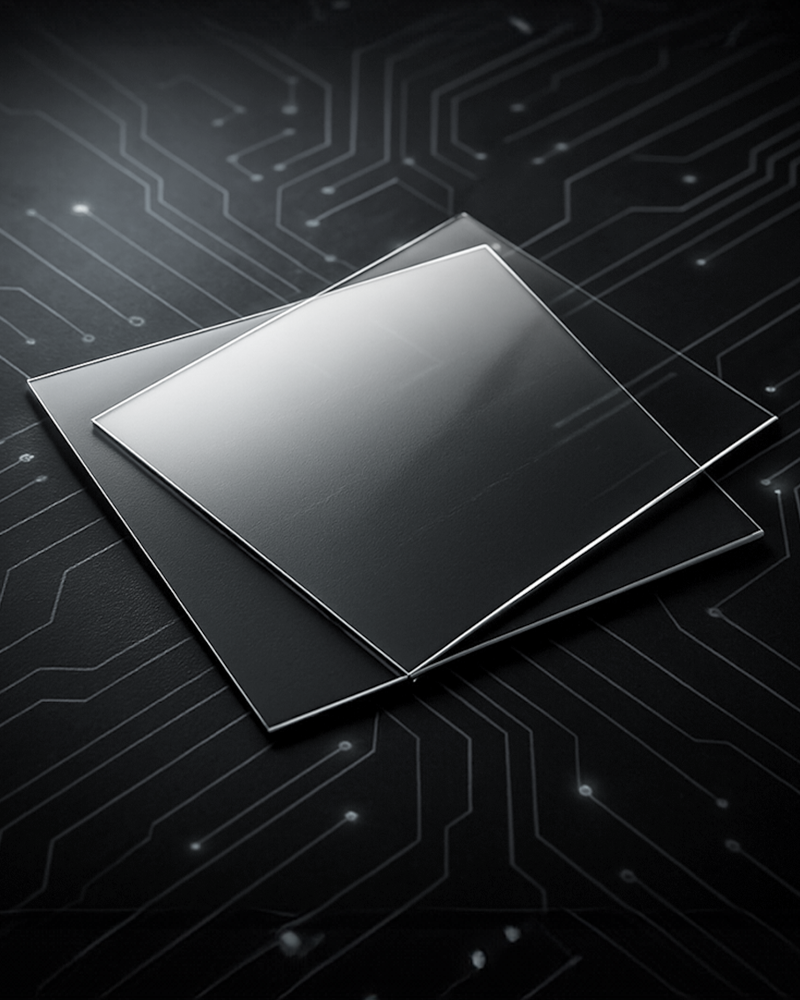
Single crystal diamond wafers represent the pinnacle of advanced material technology. Produced through a highly controlled Chemical Vapor Deposition (CVD) process, these wafers deliver outstanding crystal uniformity and minimal defect density, ensuring superior performance across a range of high-tech applications.
As a leading Single Crystal Diamond Wafers company in USA, we combine precision engineering, cutting-edge equipment, and deep material science expertise to deliver wafers that meet the evolving needs of modern industries from quantum computing and laser optics to electronics and biomedical research.
Diamond is not just the hardest known natural material; it’s also one of the most thermally conductive and optically transparent materials available. When produced as single crystal wafers, diamond’s intrinsic properties are harnessed in their purest form, making them ideal for use in:
Our wafers provide the perfect combination of mechanical robustness and electronic performance, helping industries achieve technological breakthroughs that were once thought impossible.
Every diamond wafer we produce is engineered to meet stringent performance and dimensional standards. Our products stand out for their:
Manufactured using advanced CVD techniques, our wafers exhibit near-perfect crystalline structure and minimal defects—critical for semiconductor and photonics performance.
Single crystal diamond boasts thermal conductivity exceeding 2000 W/mK, outperforming traditional materials like silicon carbide or copper, making it ideal for thermal management solutions.
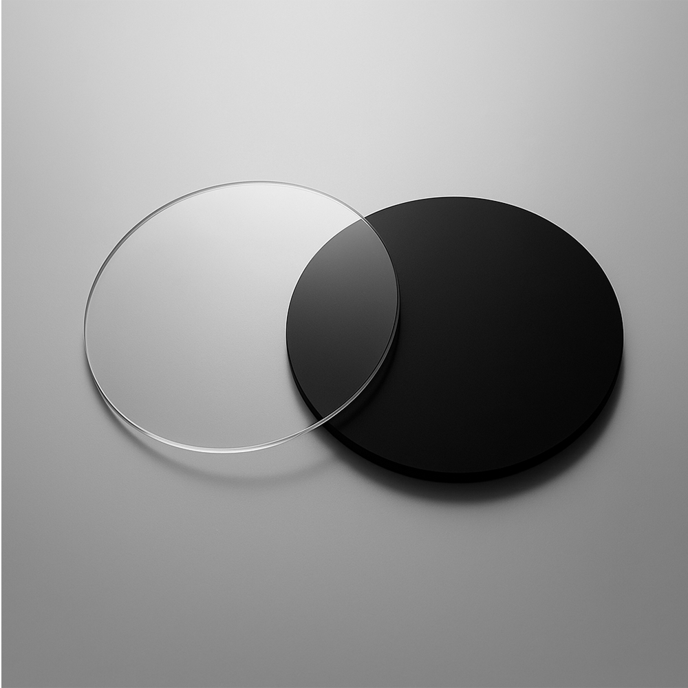
Our wafers offer broad optical transparency (UV to IR) and minimal birefringence, ensuring superior optical clarity for precision instrumentation and laser optics.
We employ advanced polishing and finishing techniques to achieve sub-nanometer surface roughness, ensuring perfect optical and electronic interfacing.
Available in various sizes, thicknesses, and orientations to meet diverse industrial needs. Whether you need a 2-inch diamond wafer or custom-shaped optical diamond plates, we deliver with precision.
Our Single Crystal Diamond Wafers in USA are trusted across multiple industries, powering cutting-edge technologies and research innovations.
Used as heat spreaders, substrates, and electronic insulators in high-performance devices. Diamond wafers enable the development of faster, smaller, and more energy-efficient components.
Our ultra-pure single crystal diamond wafers are integral for quantum devices, enabling stable NV (Nitrogen-Vacancy) centers for quantum sensing, communication, and computing.
Diamond’s resistance to laser-induced damage and thermal shock makes it ideal for high-power laser optics, infrared windows, and defense-grade optical systems.
Single crystal diamond’s biocompatibility and chemical inertness allow its use in biosensors, medical imaging, and implantable devices.
Leading laboratories and universities in the USA use our wafers for pioneering research in material science, optics, and electronics.
At Anjali Semicon, precision meets innovation in every stage of production. Here’s how we create wafers that define global quality standards:
We are more than just a manufacturer we are partners in innovation. Here’s why industry leaders trust us:
We utilize the latest CVD diamond growth systems and precision polishing tools, ensuring consistent quality and scalability.
Every application is unique. That’s why we offer tailored wafer dimensions, thicknesses, and orientations based on your specific technical requirements.
Each wafer is tested under strict quality assurance processes ensuring purity, uniformity, and performance reliability.
Based in the USA, we serve clients across North America and globally, offering quick delivery, technical support, and dedicated account management.
Our synthetic diamond wafers are ethically produced through eco-conscious manufacturing, supporting sustainability in advanced materials science.

| Parameter | Specification |
| Material | CVD Single Crystal Diamond |
| Size Available | 2mm to 50mm (custom on request) |
| Thickness | 0.1mm to 1.0mm |
| Orientation | (100), (110), (111) |
| Surface Finish | <1 nm RMS roughness |
| Thermal Conductivity | >2000 W/mK |
| Optical Range | 225 nm to 20 μm |
| Resistivity | >10¹³ Ω·cm |
Specifications can be customized based on your application.
Innovation thrives on quality, precision, and reliability and that’s exactly what we deliver. Whether you are an R&D lab pushing the boundaries of material science or a tech company developing next-generation devices, Anjali Semicon is your trusted source for Single Crystal Diamond Wafers in USA.
Our team of experts will help you choose or customize wafers that fit your application perfectly, ensuring exceptional performance and durability.
Looking for high-purity Single Crystal Diamond Wafers in USA?
Contact Anjali Semicon today for expert guidance, custom quotes, and world-class materials that power the technologies of tomorrow.
1. What are Single Crystal Diamond Wafers used for?
They are used in advanced electronics, photonics, quantum computing, optics, and biomedical devices where superior thermal, optical, and mechanical properties are essential.
2. Are these wafers synthetic or natural?
All our single crystal diamond wafers are synthetically produced using CVD (Chemical Vapor Deposition) for consistent purity and performance.
3. Can I order custom sizes or orientations?
Yes, we provide custom wafer sizes, orientations, and surface finishes tailored to your application’s needs.
4. How do Single Crystal Diamond Wafers differ from Polycrystalline Diamond?
Single crystal wafers have a uniform crystal lattice, ensuring higher optical clarity, thermal conductivity, and mechanical strength compared to polycrystalline versions.
5. Do you ship internationally?
Absolutely. We serve clients worldwide with reliable logistics and secure packaging to maintain wafer integrity during transit.